Digital Electronics Arithmetic Circuits
Adders
Adders are the combination circuit used for adding two or three one bit binary numbers. A combinational circuit is that circuit which is implemented using the boolean circuit.
Binary Addition
We are familiar with the addition of decimal numbers. Operation of binary number addition is the same as decimal number addition. Binary addition is simpler than decimal addition because in decimal numbers there are ten digits,0 to 9 digits and in binary numbers, there are only two digits, 0 and 1. The rules of binary addition are given in below table :
| Augend | Addend | Sum | Carry | Result |
|---|---|---|---|---|
| 0 | 0 | 0 | 0 | 0 |
| 0 | 1 | 1 | 0 | 1 |
| 1 | 0 | 1 | 0 | 1 |
| 1 | 1 | 0 | 1 | 10 |
In the above table, first three rows consist no carry, that is, carry=0, whereas in the fourth-row consist a carry, that is, carry=1 because largest possible digit in the binary number is 1. In decimal number addition carry is added to the next higher position.
In binary number addition, carry is added to the next higher position similar to decimal addition.
Adder Circuits
Half adder
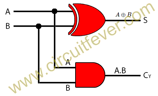
A half adder is a combination logic circuit used for addition of two one-bit binary numbers. The truth table of the half adder is given below. In the truth table, A, B are two binary inputs and S(Sum), CY(Carry) are two binary outputs.
| Input A | Input B | Output S | Output CY |
|---|---|---|---|
| 0 | 0 | 0 | 0 |
| 0 | 1 | 1 | 0 |
| 1 | 0 | 1 | 0 |
| 1 | 1 | 0 | 1 |
From the above table, Logical Expression for outputs S(Sum) and C(Carry) can be written as :
$$S=\bar {A}B +A \bar {B}=A \oplus B$$
$$C=AB$$

Full Adder
A half-adder has two inputs. When the multi-bit addition is performed, then there is no provision for adding carry coming from the lower order bit.
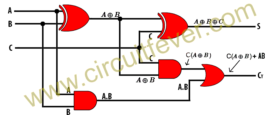
To overcome this problem, a third input terminal, C is added to this circuit. This circuit is used to add A, B, and C, where A and B are nth order bits and C is the carry generated from the addition of lower order bits.
This circuit is referred to as the full adder circuit. The truth table of the full adder is given below :
| Input A | Input B | Input C | Output S | Output CY |
| 0 | 0 | 0 | 0 | 0 |
| 0 | 0 | 1 | 1 | 0 |
| 0 | 1 | 0 | 1 | 0 |
| 0 | 1 | 1 | 0 | 1 |
| 1 | 0 | 0 | 1 | 0 |
| 1 | 0 | 1 | 0 | 1 |
| 1 | 1 | 0 | 0 | 1 |
| 1 | 1 | 1 | 1 | 1 |
From the above table, Logical Expression for output S(Sum) can be written as :
$$S=\bar{A} \bar{B}C+\bar{A}B \bar{C}+A\bar{B}\bar{C}+ABC$$
$$S=\bar{A}(\bar{B}C+B\bar{C})+A(\bar{B}\bar{C}+BC)$$
$$S=\bar{A}(B\oplus C)+A(B \odot C)$$
$$S=\bar{A}(B\oplus C)+A \overline {(B \oplus C)}$$
$$S=A \oplus B\oplus C$$
Logical expression for output CY(Carry) can be written as:
$$CY=\bar A BC+A \bar B C+AB \bar C +ABC$$
$$CY=C(\bar AB+A\bar B)+AB(C+\bar C)$$
$$CY=C(A \oplus B)+AB$$

Subtractors
Subtractors are the combination circuit used for subtracting two or three one bit binary numbers. A combinational circuit is that circuit which is implemented using the boolean circuit.
Binary Subtraction
We are familiar with the subtraction of decimal numbers. Operation of a binary number subtraction is the same as decimal number subtraction. The rules of binary addition are given in below table :
| Minuend | Subtrahend | Difference | Borrow | Result |
|---|---|---|---|---|
| 0 | 0 | 0 | 0 | 0 |
| 0 | 1 | 1 | 1 | 1 |
| 1 | 0 | 1 | 0 | 0 |
| 1 | 1 | 0 | 0 | 0 |
In the above table, the second row consists of borrow, that is, borrow=1, This borrow is subtracted from the next higher order binary bits as it is done in binary subtraction. Except for the second row, borrow=0.
Subtractor Circuits
Half subtractor
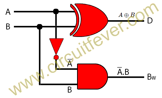
A half subtractor is a combination logic circuit used for subtraction of two one-bit binary numbers. The truth table of the half adder is given below. In the truth table, A, B are two binary inputs and D(Difference), BW(Borrow) are two binary outputs.
| Input A | Input B | Output D | Output BW |
|---|---|---|---|
| 0 | 0 | 0 | 0 |
| 0 | 1 | 1 | 1 |
| 1 | 0 | 1 | 0 |
| 1 | 1 | 0 | 0 |
From the above table, Logical Expression for outputs D(Difference), BW(Borrow) can be written as :
$$D=\bar {A}B +A \bar {B}=A \oplus B$$
$$BW=\bar{A}B$$

Full Subtractor
A half subtractor has two inputs. When the multi-bit subtraction is performed, borrow may be available from previous bit position.
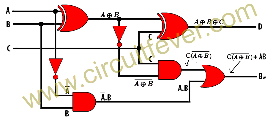
To overcome this problem, a third input terminal, C is added to this circuit. This circuit is used to subtracts A, B, and C, where A and B are nth order bits and C is the borrow from the previous stage.
D(Difference), BW(Borrow) is two outputs of this circuit.
This circuit is referred to as the full adder circuit. The truth table of the full adder is given below :
| Input A | Input B | Input C | Output D | Output BW |
| 0 | 0 | 0 | 0 | 0 |
| 0 | 0 | 1 | 1 | 1 |
| 0 | 1 | 0 | 1 | 1 |
| 0 | 1 | 1 | 0 | 1 |
| 1 | 0 | 0 | 1 | 0 |
| 1 | 0 | 1 | 0 | 0 |
| 1 | 1 | 0 | 0 | 0 |
| 1 | 1 | 1 | 1 | 1 |
From the above table, Logical Expression for output D(Difference) can be written as :
$$D=\bar{A} \bar{B}C+\bar{A}B \bar{C}+A\bar{B}\bar{C}+ABC$$
$$D=\bar{A}(\bar{B}C+B\bar{C})+A(\bar{B}\bar{C}+BC)$$
$$D=\bar{A}(B\oplus C)+A(B \odot C)$$
$$D=\bar{A}(B\oplus C)+A \overline {(B \oplus C)}$$
$$D=A \oplus B\oplus C$$
Logical expression for output BW(Borrow) can be written as:
$$BW=\bar A \bar BC+\bar A B \bar C+\bar AB C +ABC$$
$$BW=C(\bar A \bar B+AB)+\bar AB(C+\bar C)$$
$$BW+C(A \odot B)+\bar AB$$
$$BW=C(\overline {A \oplus B})+\bar AB$$

