Full Adder Verilog Code
Full adder is a combinational circuit which computer binary addition of three binary inputs. The truth table of full adder is given below and we can write boolean expression for full adder as follows $$sum = a\oplus b \oplus cin$$ $$carry = a.b + b.cin + cin.a$$
Full Adder Truth Table
Input a |
Input b |
Input cin |
Output sum |
Output carry |
|
0 |
0 |
0 |
0 |
0 |
|
0 |
0 |
1 |
1 |
0 |
|
0 |
1 |
0 |
1 |
0 |
|
0 |
1 |
1 |
0 |
1 |
|
1 |
0 |
0 |
1 |
0 |
|
1 |
0 |
1 |
0 |
1 |
|
1 |
1 |
0 |
0 |
1 |
|
1 |
1 |
1 |
1 |
1 |
Full Adder Verilog Code
Full adder has three inputs (a,b,cin) and two outputs (sum,carry). First, create a module with a module name full_adder_s as given below.
//Full adder using structural modeling
module full_adder_s ();

endmodule
Now create input output port list.
//Full adder using structural modeling
module full_adder_s (
    input a,b,cin,
    output sum,carry
);

endmodule
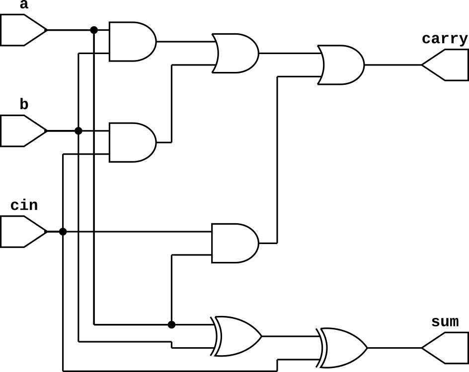
Now desciribe the hardware inside the module. Sum is a ex-or b ex-or cin and carry is a and b or b and c or c and a. We require tho ex-or gates, three and gate and one OR gate. Below is the verilog code using structural modeling because we are using logic gate instantiation only for entire hardware description. For making internal connection, we are using wire keyword.
//Full adder using structural modeling
module full_adder_s (
    input a,b,cin,
    output sum,carry
);

wire w1,w2,w3,w4;       //Internal connections

xor(w1,a,b);
xor(sum,w1,cin);        //Sum output

and(w2,a,b);
and(w3,b,cin);
and(w4,cin,a);

or(carry,w2,w3,w4);     //carry output

endmodule
Below is the Verilog code for full adder using data-flow modeling because we are using assign statement to assign a logic function to the output. We can wite the entire expression in a single line as given below.
//full adder using data-flow modeling
module full_adder_d (
    input a,b,cin,
    output sum,carry
);

assign sum = a ^ b ^ cin;
assign carry = (a & b) | (b & cin)  | (cin & a) ;

endmodule
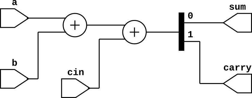
We can also use adder operator for creating full adder crcuit because full adder is basically addition of three binary inputs as given below. If we add three binary number, we will get two bit binary output. That's why we have concatinated carry and sum
//full adder using Verilog Operator
module full_adder_o (
    input a,b,cin,
    output sum,carry
);

assign {carry,sum} = a+b+cin;

endmodule
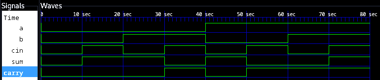
Full Adder Testbench
module full_adder_tb;
reg a,b,cin;
wire sum,carry;

full_adder_s uut(a,b,cin,sum,carry);

initial begin
a = 0; b = 0; cin = 0;
#10
a = 0; b = 0; cin = 1;
#10
a = 0; b = 1; cin = 0;
#10
a = 0; b = 1; cin = 1;
#10
a = 1; b = 0; cin = 0;
#10
a = 1; b = 0; cin = 1;
#10
a = 1; b = 1; cin = 0;
#10
a = 1; b = 1; cin = 1;
#10
$finish();
end

endmodule