How to create Block RAM On FPGA
Block RAM are the dedicated resources FPGA which we can use as a memory. We can create RAM, ROM and a memory using block RAM.
Before going to the next step, make a new project in Vivado. Select approprate board or part number while creating a project
Create a Block RAM
In Project Managet, select IP Catalog or else click Windlow -> IP Catalog
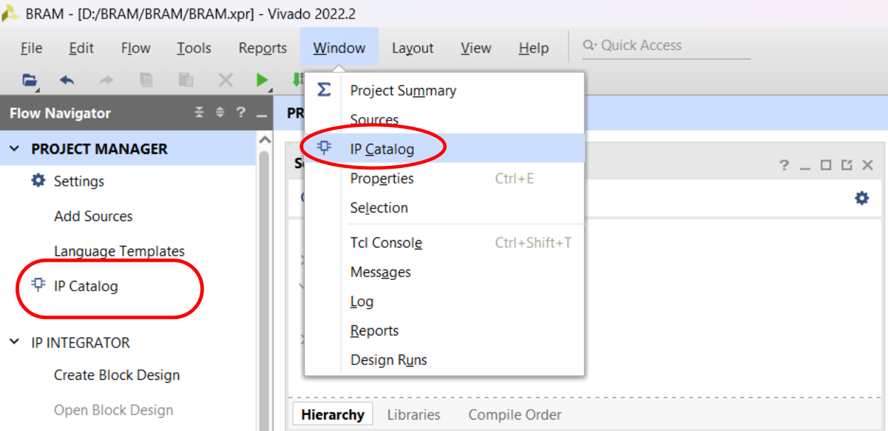
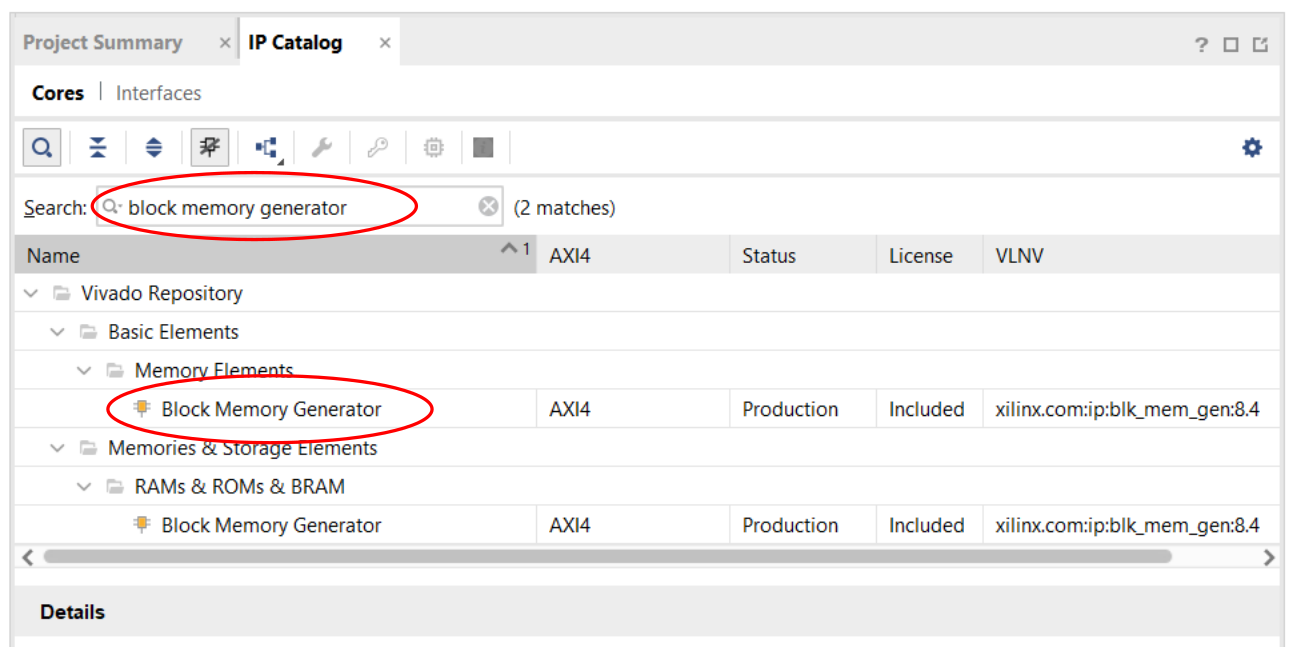
In IP Catalog window, search for Block Memory Generator and double click on Block Memory Generator.
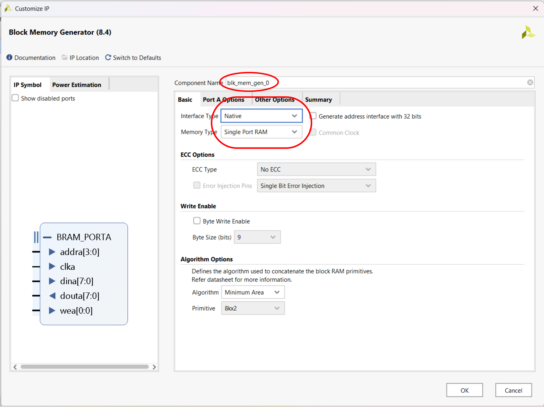
A window will open and it will looks like the window shown below. You'll find lots of options here. Using this window, we can create RAM and ROM. Select Interface Type to Native and Memory Type Single Port RAM.
Click on Port A Options and type 8 in Write Width and Read Width. Type 16 in Write Depth and Read Depth. Select Enable Port Type to Always Enable. Click OK
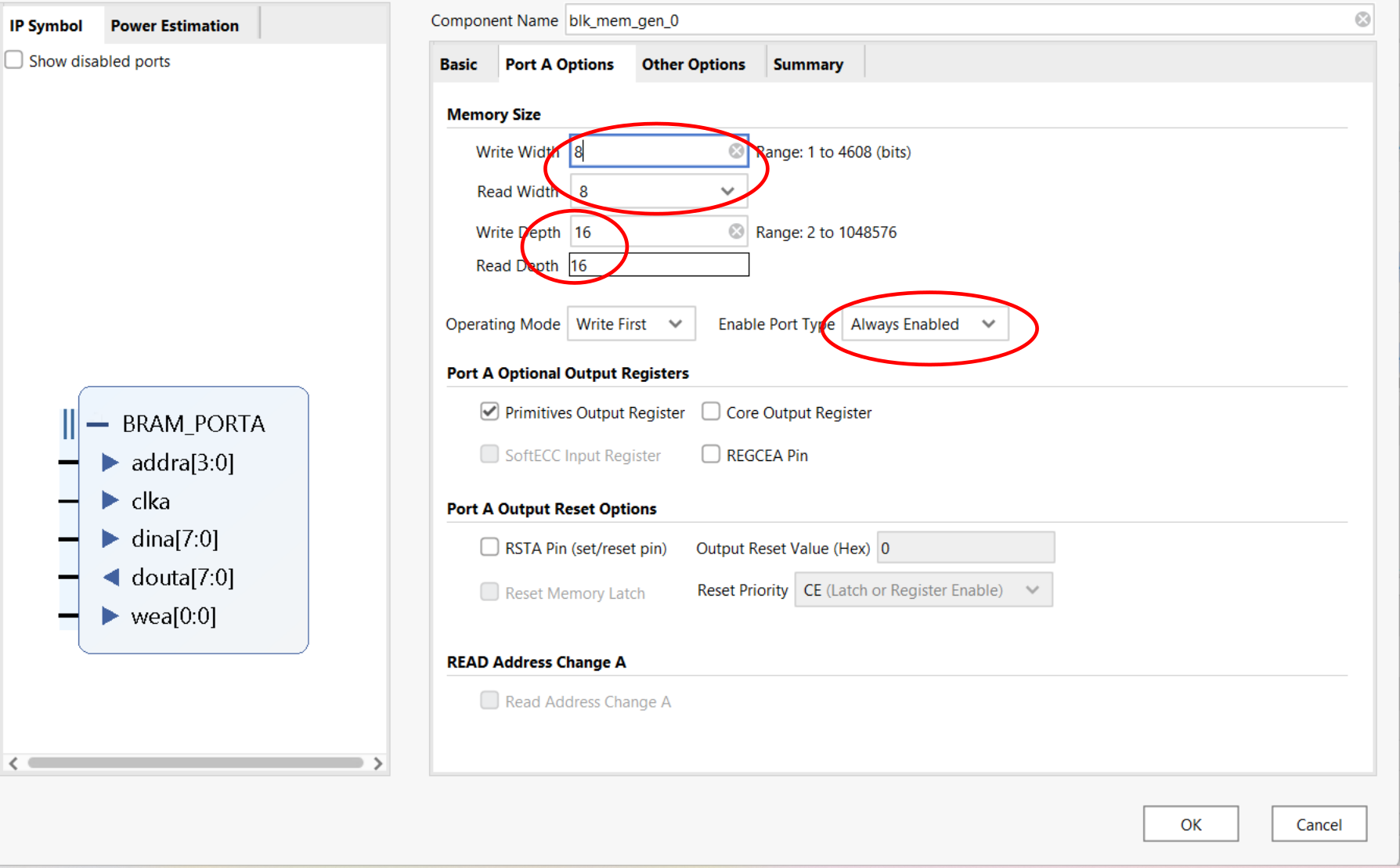
This will create a Block RAM of width 8-bit and depth 16 (Total 16 numbers of locations). For locating 16 locations, 4-bit address lines is required.
BRAM Instantiation in HDL source
We can instantiate this block RAM in both VHDL and Verilog. In most of the IP you will find example lines for instantiating IP in HDL source by clicking on IP that we've created. Some IP doesn't have example for Verilog Instantiations. But it is very simple. Just write the name of block RAM and do the port mapping.
If you see the block diagram of IP, there are 5 number of input and output ports. Clock (clka), Address(addra), Data In(dina), Data Out(douta) and Write Enable(wea).
Declare these input output ports and instantiate block RAM. The example verilog code is given below.
module bram(clk,address,data_in,data_out,write_en);

input clk;
input write_en;
input [3:0]address;
input [7:0]data_in;
output [7:0]data_out;

blk_mem_gen_0 bram(.clka(clk),.addra(address),.dina(data_in),.douta(data_out),.wea(write_en));

endmodule
Let's Simulate It
module bram_tb;

reg clk;
reg [3:0]address;
reg [7:0]data_in;
wire [7:0]data_out;
reg write_en;

bram uut(clk,address,data_in,data_out,write_en);

initial begin
clk = 0;
data_in = 8'h67;
address = 4'h5;
write_en = 0;    //Reads from address 0
#20
write_en = 1;    //Write HEX 67 to address HEX 5
#20
write_en = 0;    //Reads from address HEX 5
#20
$finish();
end

always #10 clk = ~clk;  //Creates clock of period 20 ns

endmodule
In this test bench we are first reading from randon address. We can see that the output is 0 because we have not written anyhthing into this location. After that, we are writing hex 67 into the address hex 5 and reading this back after the write operation.
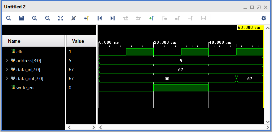
You can change the location and data and try this example. Thats it.

