
How to program Nexys4 DDR FPGA Board
In this tutorial, we'll describe a hardware (Half adder) in Verilog HDL and we'll make half adder in FPGA by programing the FPGA board. For this Tutorial we are using Nexys4 DDR FPGA board and Xilinx Vivado.
1. Describe a Hardware
Create a project in Xilinx Vivado and descibe a hardware. For example, we are using a Half Adder which is described in Verilog HDL.
module half_adder(
              input a , b,
              output sum , carry
              );

          assign sum = a ^ b;     //a ex-or b
          assign carry = a & b;   //a and b

endmodule
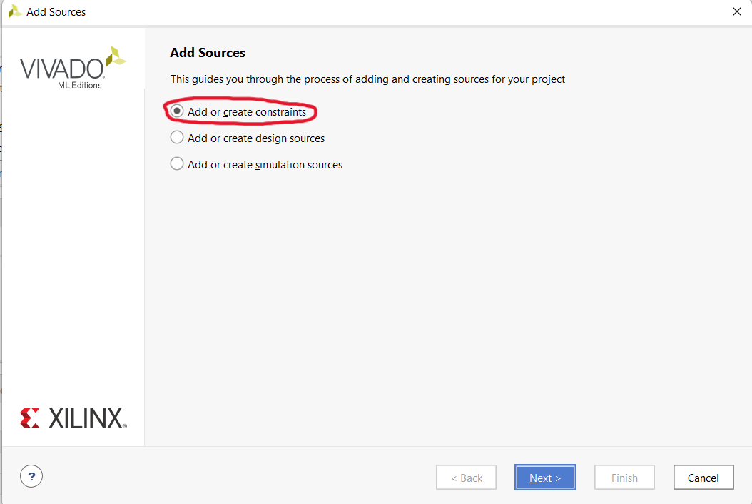
2. Create a Constraints file
For creating a Constraints file, Click on File → Add Sources → Create or Add Constraints file
Add following lines to the Constraints file
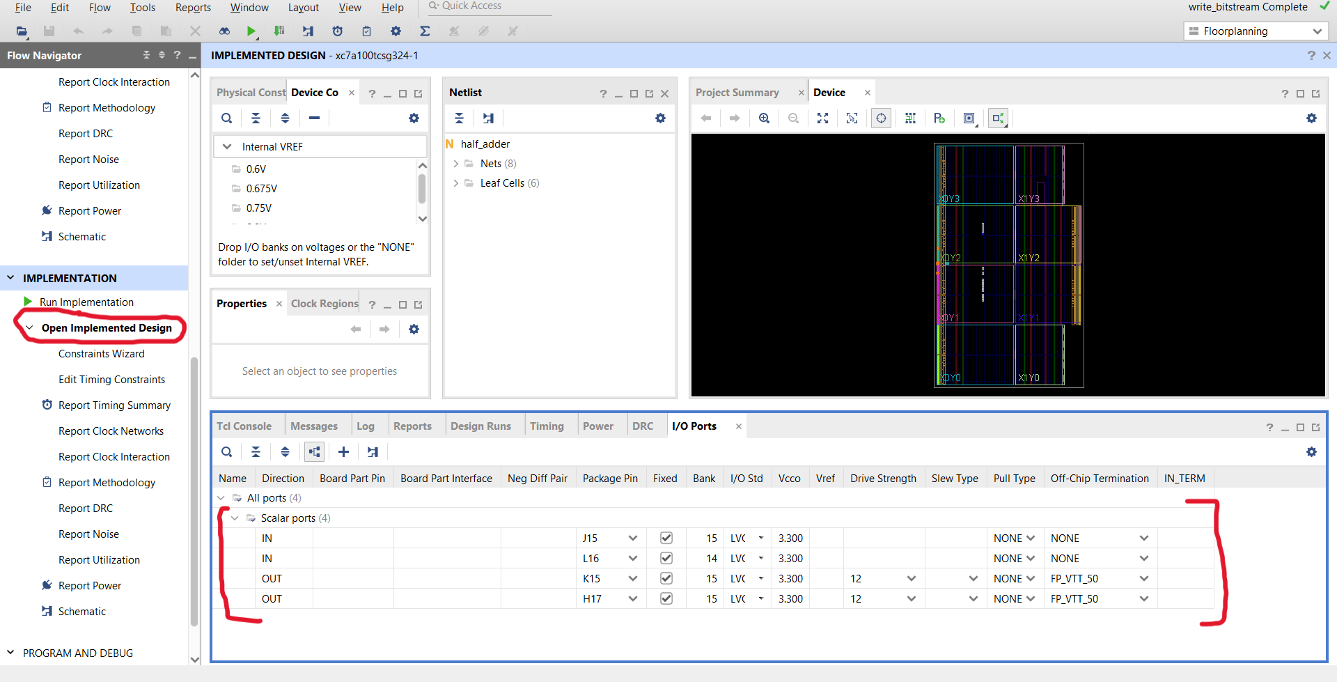
set_property -dict { PACKAGE_PIN J15   IOSTANDARD LVCMOS33 } [get_ports { a }];
          set_property -dict { PACKAGE_PIN L16   IOSTANDARD LVCMOS33 } [get_ports { b }];
          set_property -dict { PACKAGE_PIN H17   IOSTANDARD LVCMOS33 } [get_ports { sum }];
          set_property -dict { PACKAGE_PIN K15   IOSTANDARD LVCMOS33 } [get_ports { carry }];
3. Synthesis and Implementation
In FLow Navigator, Click on SYNTHESIS → Run Synthesis. After the completion of Systehesis click on IMPLEMENTATION → Run Implementation.
5. Generate Bitstream File
Click on PROGRAM NAD DEBUG → Generate Bitstream
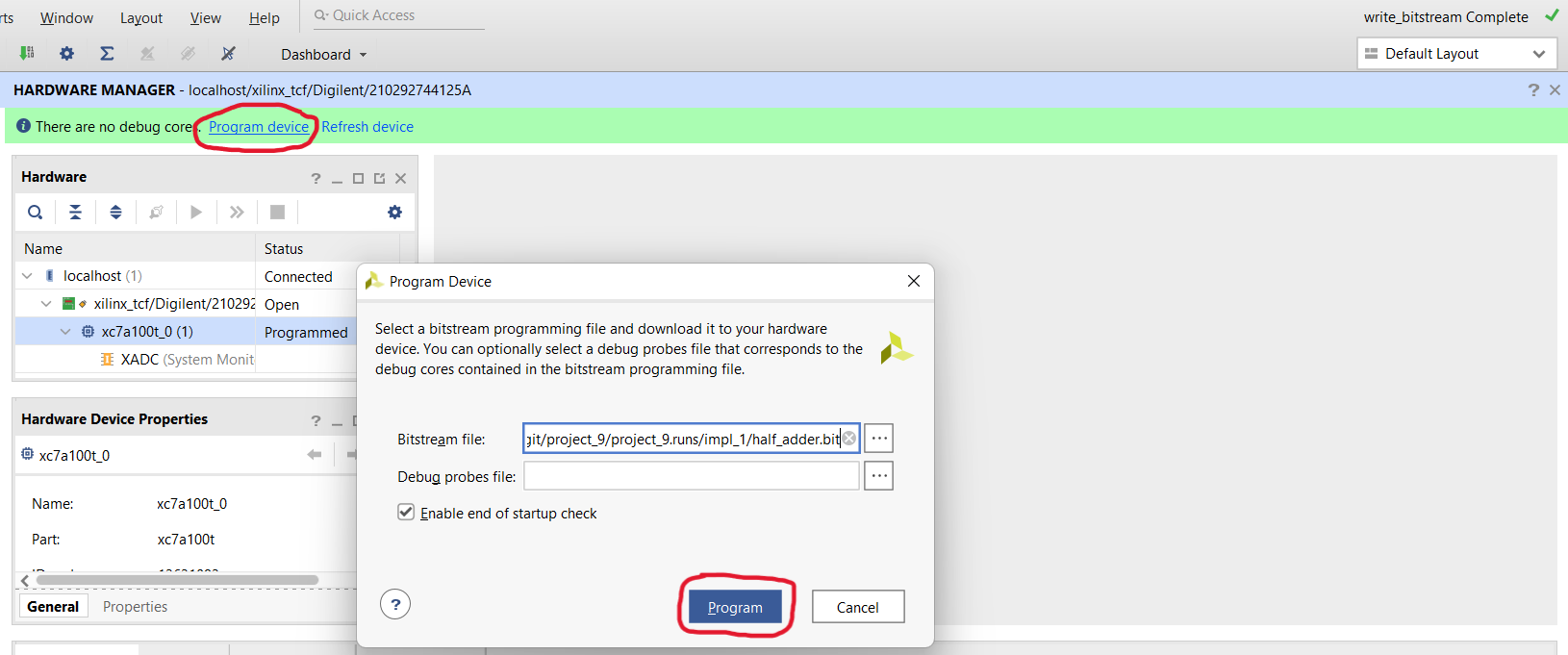
5. Program FPGA Device
Click on PROGRAM NAD DEBUG → Open Hardware Manager → Open Target → Program
0 Likes