Logic Gates Using Diodes and Transistor
Logic gates are building blocks of the digital system. In this post, we will see how basic digital gates can be made with the help of diodes and transistor.
OR Gate Using Diode
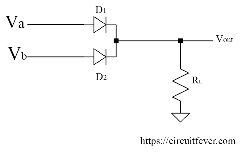
OR gate has two or more inputs and only one output. The output of the OR gate is HIGH if one or more inputs are HIGH. Circuit diagram of two input, positive logic OR gate using diodes and a resistor is shown below:

In this logic gate circuit, \(V_a\) and \(V_b\) are inputs and \(V_{out}\) is output. These symbols can take only two values either LOW or HIGH.
Working :
| Va | Vb | Vout |
|---|---|---|
LOW |
LOW |
LOW |
LOW |
HIGH |
HIGH |
HIGH |
LOW |
HIGH |
HIGH |
HIGH |
HIGH |
Let us understand the working of this circuit.
If all inputs are in LOW, both the diode becomes in reverse biased hence acts as an open switch. Hence the output voltage is LOW.
If A is HIGH and B is LOW, the diode D1 becomes in forward biased hence act as the closed switch. (Neglecting diode forward resistance and voltage drop across the diode) Hence the output is HIGH.
Also, If A is LOW and B is HIGH. Diode D2 becomes in forward biased and act as an open switch. Hence the output is HIGH.
If both the input is in HIGH then the output is equal to the more positive value of the input.
Hence OR function has been implemented.
AND gate using diodes
AND gate has two or more inputs and only one output. The output of logic AND gate is HIGH if all inputs are HIGH. For other input, the output is LOW.
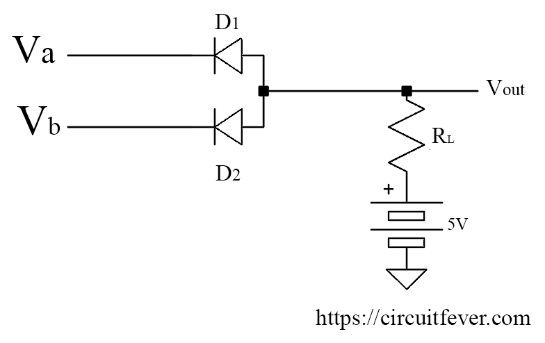
Circuit diagram of two-input AND gate using diodes and a resistor is shown below:

Here \(V_a\) and \(V_b\) are inputs and \(V_{out}\) is output.
Working :
| Va | Vb | Vout |
|---|---|---|
LOW |
LOW |
LOW |
LOW |
HIGH |
LOW |
HIGH |
LOW |
LOW |
HIGH |
HIGH |
HIGH |
If A is HIGN and b is LOW, the diode D1 becomes in reversed biased hence act as an open switch. Also, diode D2 becomes in forward biased hence act as the closed switch. Hence the output is LOW.
If A is LOW and B is HIGH, the diode D1 becomes in forward biased hence act as the closed switch. Also, diode D2 becomes in reversed biased hence act as an open switch. The output is LOW.
If all inputs are LOW then all diode becomes in forward biased and act as an open switch. Hence the output is LOW.
When all inputs are HIGH then all diodes becomes in the reversed biased hence act as an open switch. Hence the output is HIGH.
NOT gate using a transistor
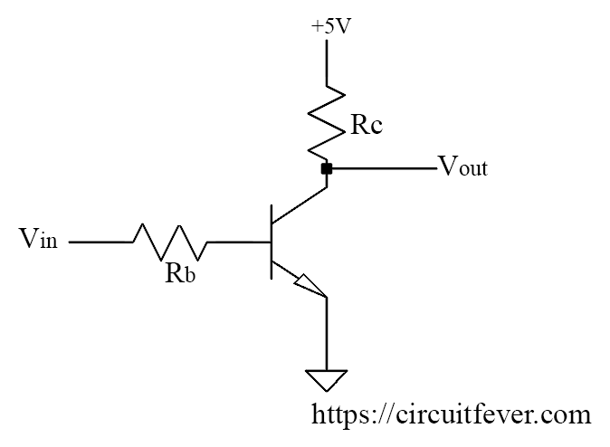
NOT gate It is also known as an inverter because the output is opposite to the input. It has one input and one output. Circuit diagram of NOT gate using transistor is shown below:

Here, \(V_{in}\) is input and \(V_{out}\) is output. Output must be LOW if the input is HIGH. Also, the output must be HIGH if the input is LOW.
Working:
| Vin | Vout |
|---|---|
LOW |
HIGH |
HIGH |
LOW |
If the input is LOW, the parameter is chosen so that the output is V(sat). Also, if the input is HIGH, the parameter is chosen so that the output is LOW.
If the input is LOW, the transistor act as an open switch. Hence the output is HIGH.
If the input is HIGH, the transistor act as the closed switch. Hence the output is LOW (Neglecting voltage drop).

