Random Access Memory (RAM) Verilog Code
Random Access Memory is the temporary memory used in a processor or the digital system which requires larger memory for storing temporary data. When designing any system on FPGA, sometimes we require a RAM block which is also called BRAM or block RAM. In this post, we'll how to describe a RAM in Verilog HDL. Most of the latest FPGAs have BRAM and if we synthesize this, it will be synthesized into a BRAM
Verilog Code
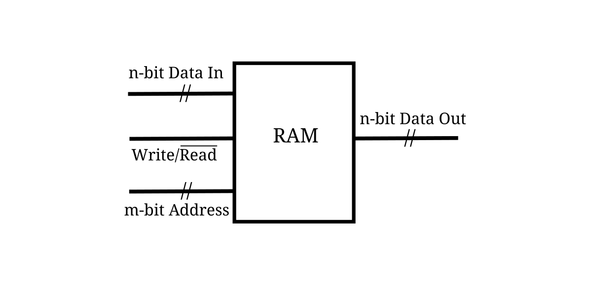
A RAM has a data bus (sometimes called width of RAM) form which we can access content from the RAM or we can put a content on this, and if we give write command to the RAM, it'll write RAM with the content on the data bus. RAM has lots of addresses (sometimes called depth of RAM) and these addresses can be accessed by the address bus.
Other than data and address bus, RAM has one more input read/write. If it's state is changed, let's say if it is high, the content at data bus is written to the address provided to the RAM from address bus else the content of the address provided by address bus is reflected to the data bus.
Below is the code of 1 kilo byte RAM describe using Verilog HDL. The width of the RAM is 8-bit and depth is 1024 (which is 1 kilo). For making the code simple, there are two similar data bus, one will be used to read the content from the RAM and another is used to provide content to the data bus and, when read write input is high, this content is written to the address of the RAM
//1 kilo byte Random Access Memory
module ram(
    input clk,
    input write_enable,
    input [9:0]address,
    input [7:0]data_in,
    output reg [7:0]data_out
);

reg [7:0]ram_block[0:1023];

always @(posedge clk) begin
        if(write_enable)
            ram_block[address] <= data_in;
        else
            data_out <= ram_block[address];
end

endmodule
Below is the block diagram of a RAM. Note that data bus data_in and data_out are of same size because it needs to be similar. The RAM may have more inputs like RAM enable, you can try to make this.
RAM Testbench
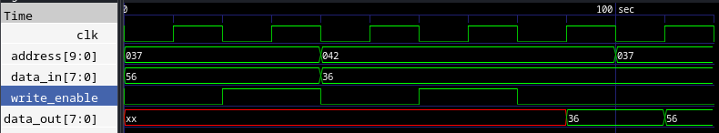
In the testbench given below, we are writing some content to the few location of the RAM and then we are reading back the written data form the same location. If we are able to write and read, everything is fine and this will be synthesized to BRAM of the FPGA (if FPGA have BRAM).
module ram_tb;

reg clk;
reg write_enable;
reg [9:0]address;
reg [7:0]data_in;
wire [7:0]data_out;

ram uut(clk,write_enable,address,data_in,data_out);

initial begin
clk = 0;
data_in = 8'h56;
write_enable = 0;
address = 55;
#20
write_enable = 1;
#20;
write_enable = 0;
address = 66;
data_in = 8'h36;
#20
write_enable = 1;
#20
write_enable = 0;
#20
address = 55;
#20
$finish();

end

always #10 clk = ~clk;  //clock generation

endmodule
Below is the output waveform of the above testbench and RAM Verilog code. If you see the output waveform, read or write is reflecting at only a single clock cycle. It may not always true because the RAM has read/write delay which may be more than one clock cycle. If the implementation of this verilog code is not working on FPGA, try to increase the clock cycle. For example, if the read/write delay is 2 clock cycles, read write input should be high for at least 2 clock cycle if there is a write operation and vice versa.