Seven Segment Display Decoder In FPGA using Verilog
Seven segment display is one of the basic display used in some of the electronic devices for displaying numbers like in basic calculators, there are seven segment displays which shows the number entered by the user of the output of the calculation perforem by in input given by the user. It has seven display unit (excluding dot) display unit can by an led or liquid crystals which has two states when used as a basic display display. We can display decimal numbers (0-9) or hexadecimal numbers (0-9,A,B,C,D,E,F) on this.
If we want to represent single digit decimal or hexadecimal numbers, we require 4 binary number but seven segment display has seven inputs and for displaying some number we should give some input pattern to the display like for displaying digit 1, b and c segment should be on. For this we require a decoder which takes 4-bit number as and input and generate 7-bit pattern which is required to display that particular number. The complete seven segment pattern can be found here..
In this block post we'll learn how to make a decoder for a seven segment display. Most of the FPGA development board has seven segment display we can use that for this implementation. If not then you can use external seven segment display and connect that with the PMOD connector.
What we require?
- A FPGA Board
- A Synthesis tool (Vivado)
- USB Cable
- Seven Segment Display (If it is not available in the board)
How to make?
Decoder is a combinational circuit which has m-bit inputs and n-bit outputs. Seven segment display decoder has 4-bit inputs and 7-bit outputs (8-bit if we include the dot). We'll describe the decoder code in Verilog FPGA and implement this on FPGA. We'll give input number by using switch and observe the output of the display.
Verilog Description
The complete Verilog code for seven segment display for common anode (LED will glow if we give logic 0 to the segment) is given below. If you have common anode just change 0 to 1 and 1 to 0. Also, make sure to check logic 0 is for enable or logic 1 is for disable the seven segment display. The board I am using has active low enabled display. Change the Verilog code according to your FPGA board.
module seg7(
    input [3:0]data_in,
    output reg [7:0]display_out,
    output [7:0]AN
    );

assign AN = 8'b11111110;

always @(*) begin
    case (data_in)
        4'b0000:
            display_out = 8'b00000011;  //a,b,c,d,e,f,g,dot (zero)
        4'b0001:
            display_out = 8'b10011111;  //one
        4'b0010:
            display_out = 8'b00100101;  //two
        4'b0011:
            display_out = 8'b00001101;  //three
        4'b0100:
            display_out = 8'b10011001;  //four
        4'b0101:
            display_out = 8'b01001001;  //five
        4'b0110:
            display_out = 8'b01000001;  //six
        4'b0111:
            display_out = 8'b00011111;  //seven
        4'b1000:
            display_out = 8'b00000001;  //eight
        4'b1001:
            display_out = 8'b00001001;  //nine
        4'b1010:
            display_out = 8'b00010001;  //A
        4'b1011:
            display_out = 8'b11000001;  //b
        4'b1100:
            display_out = 8'b01100011;  //C
        4'b1101:
            display_out = 8'b10000101;  //d
        4'b1110:
            display_out = 8'b01100001;  //E
        4'b1111:
            display_out = 8'b01110001;  //F
    endcase
end
endmodule
In this Verilog description, we are using behavioural modeling for describing the decoder. We have declared 4-bit input and 8-bit output. There is another 8-bit output AN which is used to enable the ony one digit of the seven segment dislay. If you have only one seven segment, you can change it't bit width to one bit.
We have used case statement here. Each 4-bit input has its equivalent output pattern. We have used 16 statement to display hexadecimal numbers. You can change this to decimal number (only ten case) or you can make your own pattern by changing output bits of any of the case statement.
FPGA Implementation
After the Verilog code, make the connection between input output ports and the seven segment dispaly. If your FPGA baord have seven segment display then create a constraint file and make connection between your design and pins of seven segment display. After the connection, do the synthesis and generate bitstream and program the FPGA board.
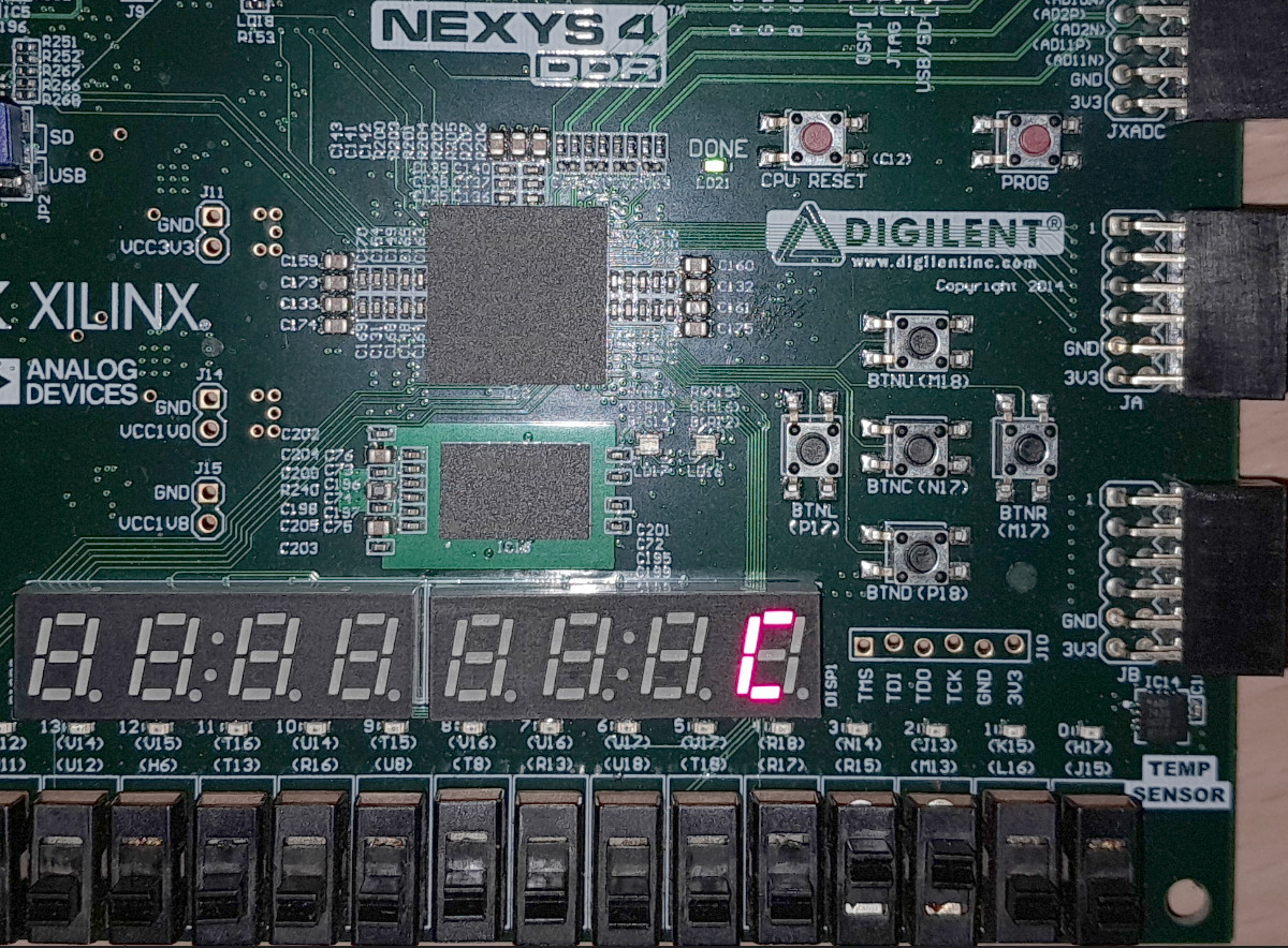
I am using Nexys 4 DDR FPGA board and it has 8-digit seven segmant display bit I am using only one by disabling rest 7 digits by giving logic 1 to its common pin. The 4-bit input is connected to the first four switch of the FPGA board.